
There aren’t many components in electronics that enjoy the same level of iconic status as the 555 timer. This is despite – or perhaps even because of – this widely used integrated circuit (IC) being so cheap; you can get one for potentially less than 50p from some suppliers.
Since its introduction by the Signetics Corporation in 1972 – built to a design by engineer Hans Camenzind (1934-2012) – the 555 timer has been used to power everything from simple LED blinkers to complex pulse generators.
The 555 Timer IC: A Highly Accessible and Versatile Component
As we touched on above, the 555 timer IC is extremely affordable. No less crucially, however, this versatile device provides a forgiving pathway into analogue circuit design for a broad range of people, including students, hobbyists, and inexperienced makers.
Understandably, though, if you’re one of those people seeking to instigate 555 timer-based circuit design projects, you might be unsure where to start.
In this article, then, we will set out some essentials to act as a launchpad for whatever kind of work you may have in mind.
How Does The 555 Timer Work?
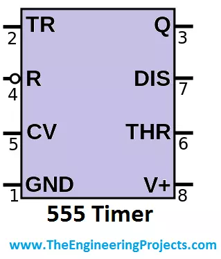
The 555 timer IC is an eight-pin integrated circuit built around two comparators, an SR (set and reset) flip-flop, a discharge transistor, and a voltage divider.
The internal voltage divider is made up of three five-kiloohm (5 kΩ) resistors, which give the 555 timer its name. This creates reference voltages at 1/3 Vcc and 2/3 Vcc, where Vcc is the supply voltage. The two comparators compare external output voltages to these references, and their outputs control the flip-flop, which in turn sets the state of the output pin (Pin 3).
An external resistor-capacitor (RC) network is typically used to control the circuit’s timing or frequency.
Basics of the 555 Timer IC’s Pin Configuration
To use the 555 timer for circuit design purposes, you will need to know what each of the eight pins is for within this device:
- Pin 1 (GND): connects to the negative supply rail (ground)
- Pin 2 (Trigger): starts the timing cycle when its voltage drops below 1/3 Vcc
- Pin 3 (Output): the main output pin, which can source or sink up to 200mA of current
- Pin 4 (Reset): an active-low input that forces the output to turn off. It should be tied to Vcc for normal operation
- Pin 5 (Control Voltage): provides access to the 2/3 Vcc reference. In a standard 555 timer configuration, this pin is left open or connected to ground via a small capacitor
- Pin 6 (Threshold): ends the timing cycle when its voltage exceeds 2/3 Vcc
- Pin 7 (Discharge): connects an internal transistor’s collector to ground, used to discharge the external timing capacitor
- Pin 8 (Vcc): connects to the positive power supply (typically between 4.5V and 15V).
The Operating Modes and Circuit Design Basics for the 555 Timer IC
The 555 timer IC can be configured to operate in the following three primary modes:
- Monostable Mode (One-Shot Timer)
In this mode, the 555 timer generates a single output pulse of a specific duration in response to a trigger, before returning to its stable state.
Typical applications for this mode include time delays, switch debouncing, and missing pulse detection.
- Astable Mode (Oscillator)
In this configuration, the 555 timer operates as a free-running oscillator. The device produces a continuous series of pulses, oscillating between high and low states without a stable state.
You might turn to this mode for such applications as LED flashers, tone generators, and clock signals.
- Bistable Mode (Flip-Flop/Latch)
This mode has two stable states: high output and low output. A button press or another trigger can be used to switch between these two states.
Common applications for this mode include toggle switches and memory elements.
Use Well-Chosen Tools to Get More from Your 555 Timer Circuit Designs
To design successful projects involving a 555 timer IC, you can expect to require certain software tools for design and simulation, as well as hardware for physical prototyping:
- Software
The right online calculator will help you determine the necessary resistor and capacitor values, so that you can achieve your desired frequency or time delay for stable or monostable modes.
You can simply log onto the website of the electrical component supplier RS, for instance, and explore the 555 timer calculator to configure pulse width and frequency.
Circuit simulator software, too, can be greatly useful for building and testing your circuit virtually, before you commit to using physical components.
- Hardware
A breadboard will be essential for building and testing circuits easily without soldering.
Core hardware components of a 555 timer IC-based circuit design include – of course – the 555 timer itself, as well as resistors, capacitors, and jumper wires.
A power source will be needed, too. A 9V battery with a battery clip or a lab power supply is a common choice for powering simple 555 timer IC circuits.
What’s Next for Your Learning Journey in Relation To 555 Timer Circuit Design?
Through the careful selection of the appropriate external resistors and capacitors, you will be able to tailor the 555 timer’s operation to any of a broad array of projects.
For more detailed information, including specific project schematics and design tools, you can seek out various resources online.
The Instructables website, for instance, offers this tutorial for the creation of 555 timer circuits in monostable, astable, and bistable modes.